
Arm presented AGI at Hot Chips on 24 August: its first in-house commercial data-centre CPU, production silicon rather than a licensed diagram. Up to 136 Neoverse V3 cores on two TSMC N3P chiplets. Clocks reach 3.7 GHz on the 64-core SKU. Arm's table lists the 136-core part at 3.5 GHz. The package is 300 watts.
Saurabh Pradhan and Deepak Goel walked the floorplan. Each chiplet holds 70 V3 cores. Extra cores sit in the hardware for harvesting, so the product that ships is 136, 128, or 64. Private L2 is 2 MB per core. System-level cache on Arm's product page is 128 MB. Memory is 12-channel DDR5, up to DDR5-8800. I/O is 96 lanes of PCIe 6.0 with CXL 3.0. Die-to-die is UCIe, Arm quoting 2 TB/s.
The Hot Chips programme put their names on the talk: "Arm AGI : A Disaggregated, Chiplet-Based Server SoC for scalable coherency and memory Bandwidth in the Terabyte/s Era." Tom's Hardware filed the 24 August session as the week Arm filled the gaps it had left at the March launch — configurations, clocks, the fact that the silicon works as planned, commercial shipments still listed for late 2026. ServeTheHome had the same session in the second CPU block of the day. Partners have been shipping Arm cores for years. On 24 August Arm walked a finished processor.
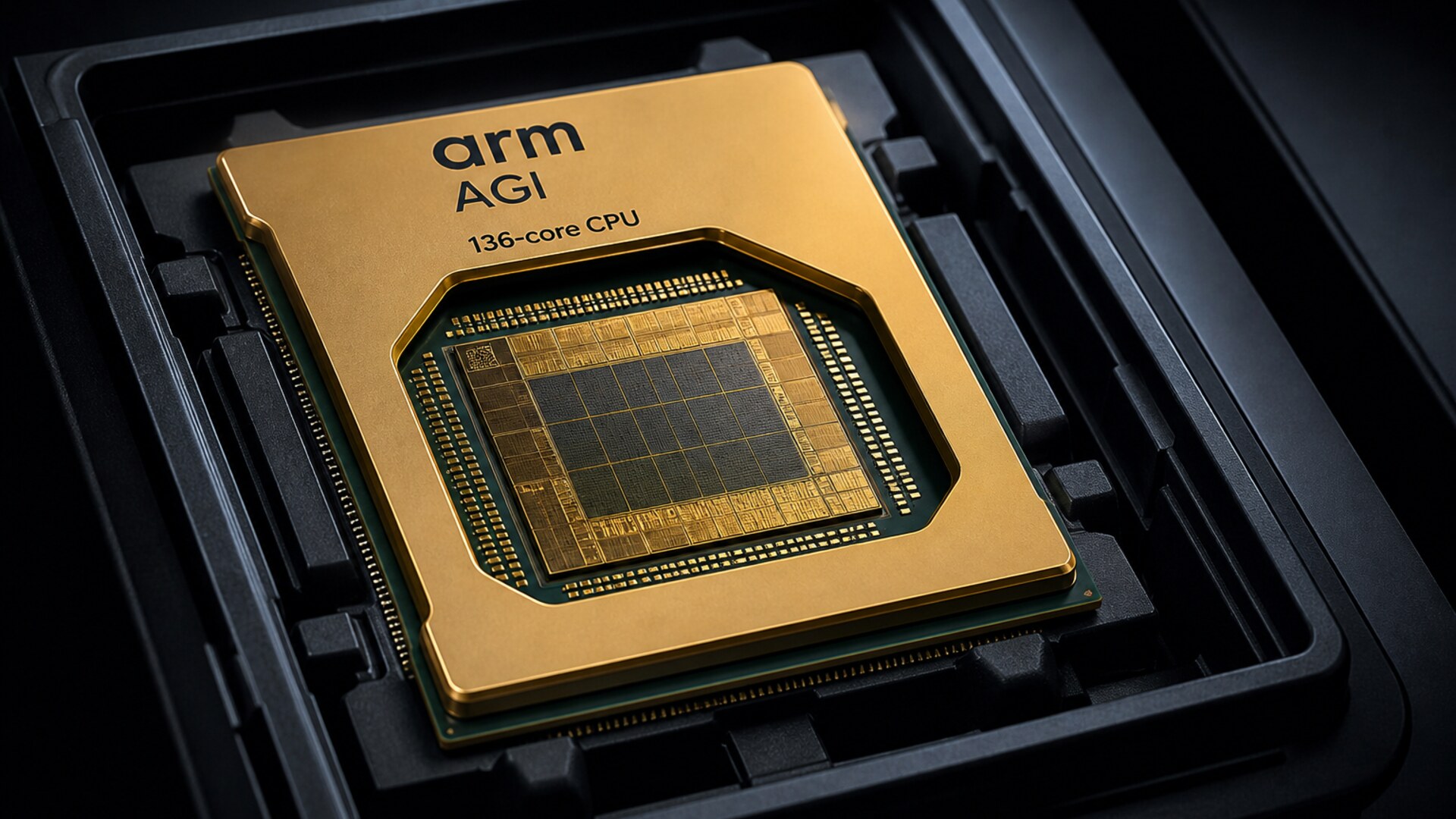
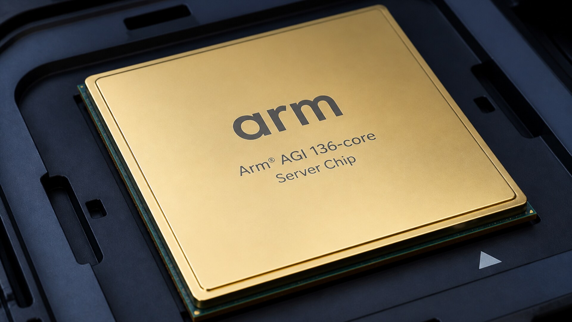
SKUs are named like a parts list. SP113012 is 136 cores. SP113012S is 128. SP113012A is 64. Two sockets. Two DIMMs per channel. Compute and memory controllers live on the same chiplet. That is the design choice Tom's Hardware flagged against AMD, Intel, and now Nvidia, who separate compute and I/O. Arm put two largely self-contained SoC chiplets on TSMC N3P and tied them with UCIe. Each chiplet is more than 50 billion transistors. XenoSpectrum added the two-chiplet total past 100 billion. Each chiplet carries 70 Neoverse V3 cores. Two times 70 is 140. The top SKU enables 136. Four cores sit in the hardware for yield. ServeTheHome wrote 144 in hardware in one line; 70 plus 70 is 140. The count is 70 per chiplet, harvest down to 136, 128, or 64, which is how Pradhan and Goel walked it. The gold spreader in the tray is printed Arm AGI 136-core Server Chip. That is the product, not the recipe.
Clocks are a 300 watt conversation. The 136-core part: 2.8 GHz typical, 3.2 GHz base, 3.5 GHz boost on XenoSpectrum's table of the slides. The 128-core TCO SKU: the same 2.8 / 3.2 / 3.5. The 64-core max-memory SKU: 2.8 / 3.5 / 3.7. Private L2 scales with cores — 272 MB total on the 136, 256 MB on the 128, 128 MB on the 64. System-level cache stays 128 MB across all three. Arm's product page is the 128 MB SLC used here. Memory bandwidth per core on that same slide table is about 6 GB/s on the 136, 6.3 on the 128, 13 on the 64. Twelve-channel DDR5-8800. Tom's Hardware put up to 3 TB per chiplet and 6 TB per socket. I/O is 96 lanes of PCIe 6.0 with CXL 3.0, plus four lanes of PCIe 4.0, plus I3C, I2C, and SPI. Die-to-die is 16 × 16 UCIe macros at 32 GT/s, Arm quoting 2 TB/s aggregate. The 64-core SKU is the one that clocks to 3.7 GHz. The 136-core SKU is the one that fills the tray.
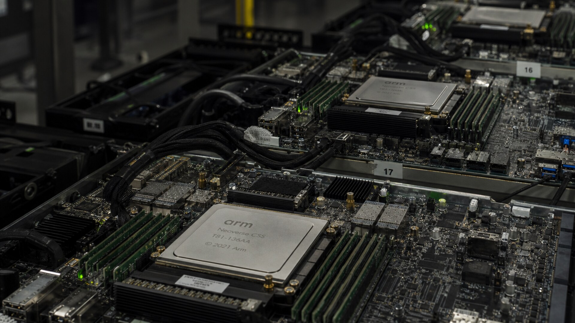
The V3 core is a 10-wide frontend and decode, 10-wide dispatch, 8-wide retire, 384-plus entry out-of-order window, two 128-bit vector engines, 2 MB of L2, 64 KB instruction and 64 KB data L1. ServeTheHome called it a balance part, a minimum single-thread target, not a frequency trophy. Arm picked TSMC N3P because it is a proven performance node. The undertext, as ServeTheHome wrote it, is that Arm did not want N2 for this first finished chip. The job on the slide is agentic AI servers: a host that can orchestrate accelerators. Arm's page calls it production silicon for that work. Server designs already on the board include Supermicro, Lenovo, and ASRock Rack. Commercial shipments are listed for late 2026. The rack photograph is the board version of that sentence: an Arm Neoverse CSS part marked T81-136AA, DIMMs left and right, a finned heatsink below the socket, mesh-sleeved cables, green LEDs, chassis labels 17 and 16.
March was the launch. 24 August was the floorplan. Tom's Hardware noted that Arm had omitted a performance table in March and still did not put a SPECrate on the Hot Chips slides. The missing bench stays missing. What 24 August added is the 70-core chiplet, the harvest math, the 2 TB/s UCIe number, the 12-channel DDR5-8800, the 96 lanes of PCIe 6.0, the 300 watt envelope, and the three SKU names. SP113012, SP113012S, SP113012A. Two sockets. Two DIMMs per channel. More than 50 billion transistors per chiplet. 128 MB of system-level cache on the product page. 2 MB of L2 per core. 3.7 GHz on the 64-core. 3.5 GHz on the 136. Late 2026 for commercial crates.
Memory is the other half of a 300 watt host. Twelve channels, DDR5-8800, two DIMMs per channel, up to 3 TB on a chiplet and 6 TB on a socket in Tom's Hardware's read of the slides. The 64-core SKU exists so that memory per core can double. 13 GB/s per core on the 64 against 6 GB/s on the 136 is the reason Arm printed three products at the same wattage. XenoSpectrum's SKU table is the source of those per-core bandwidth figures. SLC does not grow when you buy more cores. 128 MB is 128 MB on SP113012, SP113012S, and SP113012A. L2 is the thing that scales: 2 MB times 136 is 272 MB, 2 MB times 64 is 128 MB. Anyone shopping the 64-core part for a memory-heavy agentic host is shopping the 3.7 GHz boost and the fatter channel per core, not a smaller package. The package is still 300 watts.
UCIe is how the two N3P chiplets pretend to be one socket. Sixteen by sixteen macros at 32 GT/s, 2 TB/s quoted. Compute and the memory controllers sit on the same die, so a load that stays on one chiplet does not have to cross the fabric to find DRAM. A load that spans both chiplets does. That is the disaggregated SoC in the talk title. It is also why Arm did not follow the I/O-die fashion for this first finished chip. N3P for both halves. More than 50 billion transistors each. Harvest four cores so a 140-core pair of dies can ship as 136. Ship 128 if the yield wants a TCO SKU. Ship 64 if the customer wants clock and memory. Late 2026 is still the commercial line. Supermicro, Lenovo, ASRock Rack are still the three boards named.
Arm has sold IP since the 1990s. Neoverse V3 is already in other people's silicon. AGI is Arm selling the socket. The next number is a two-socket crate when one of those three vendors ships one. Until then the news is the 24 August package: 136 Neoverse V3 cores, two TSMC N3P chiplets, 300 watts, a gold spreader that says Server Chip, and a company that used to license the diagram now quoting 2 TB/s of UCIe on a part you can put in a tray. Pradhan and Goel walked that floorplan. The tray and the rack are the photographs. The SKU is SP113012. The year on the shipment line is still 2026.
The gold spreader says Server Chip. The board in the rack says Neoverse CSS T81-136AA. Those are two photographs of the same move: Arm selling a finished processor, not a PDF of a core. 136 Neoverse V3 cores. Two TSMC N3P chiplets. 300 watts. 12-channel DDR5-8800. 96 lanes of PCIe 6.0. 2 TB/s of UCIe. SP113012 in the tray. Late 2026 on the shipment line. Supermicro, Lenovo, and ASRock Rack on the design-win list. File a SPECrate when Arm prints one.
The paper
Comments
No notes on this story yet.
Sign in to comment