
Fujitsu took Monaka to Hot Chips on 24 August and said the quiet hardware out loud. One hundred and forty-four Armv9.3-A cores. Dual 256-bit SVE2 on each, down from the 512-bit SVE on A64FX. The last-level cache lives on its own 5 nm die. The cores sit on TSMC N2P, stacked face-to-face through hybrid bonding, on the cool side because they run hottest. The I/O die is 5 nm too, across an interposer.
Ryohei Okazaki, who leads the processor team, called it a made-in-Japan CPU for AI performance and power, built for what Fujitsu calls green AI data centres and backed by NEDO. Two SKUs, both 144 cores. Air-cooled 350 W at a 2.1 GHz base. Liquid-cooled 500 W at 2.9 GHz, about 50 percent more performance on Fujitsu's own estimate.
Tom's Hardware, filing Luke James on 26 August, put Okazaki's line in English: "a made-in-Japan CPU, specifically engineered for AI performance and power efficiency." ServeTheHome had him in the second CPU session of the day. The Hot Chips programme named the talk "Next-Generation Arm-based CPU FUJITSU-MONAKA for green AI data center." Evaluation samples are out now. Volume production is 2027. Fujitsu has not published a price. The 2027 board will be the news when a vendor ships one.
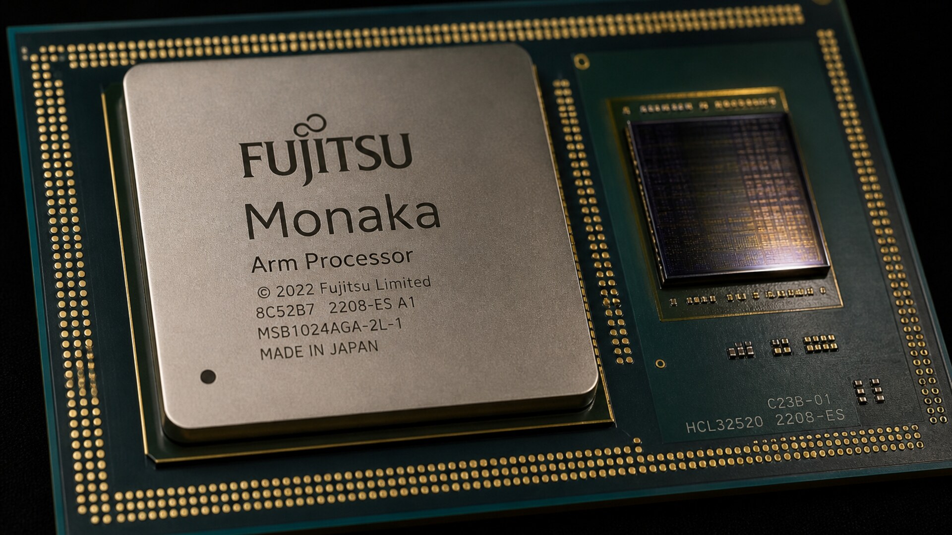
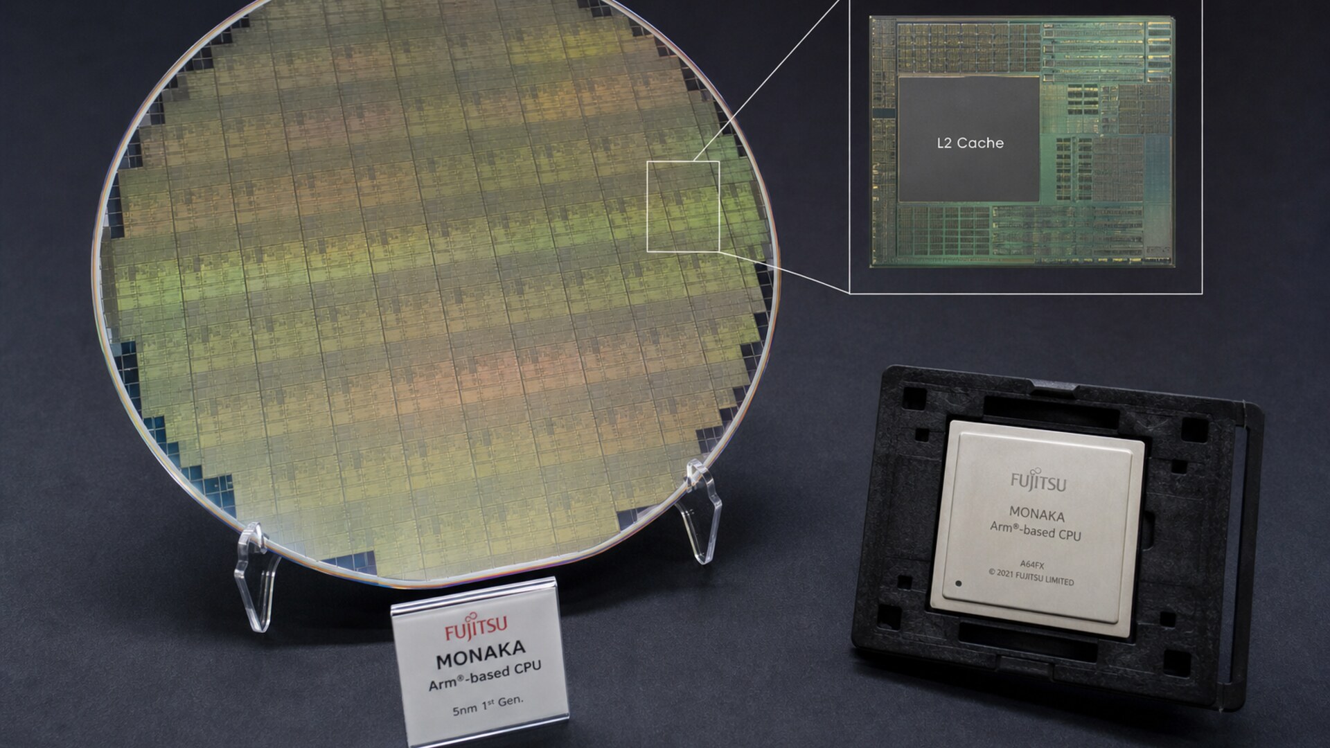
Monaka splits into three tiers of silicon. A 2 nm core die on TSMC N2P. A 5 nm SRAM die on TSMC N5 that holds the whole last-level cache. A 5 nm I/O die. The core die stacks face-to-face on the SRAM die through hybrid bonding, sitting on the cooling side because it runs hottest. The I/O die meets the SRAM die across a silicon interposer. Fujitsu keeps 2 nm under 30 percent of total die area on purpose. Okazaki said that split lets Fujitsu "accelerate the time to market for our 2-nanometer-based chip" by pushing what shrinks poorly onto the 5 nm SRAM and I/O dies. Low-dropout voltage regulators moved onto the 5 nm SRAM die because analog does not love 2 nm, and they sit under the floating-point units to feed per-core DVFS. Tom's Hardware lined the cache stack up with Intel's Clearwater Forest, where local cache sits in a base tile with compute above, and away from AMD's 3D V-Cache, which bonds extra SRAM onto a compute die that already has L3. The wafer in the photograph is the 5 nm sentence made visible: a placard reading FUJITSU MONAKA Arm-based CPU, 5nm 1st Gen, an inset labelled L2 Cache, a packaged part in a black tray. The heat spreader on that tray still carries A64FX in the engraving, the 7 nm predecessor that powered Fugaku. The engraving is heritage on a sample package, not the 2026 floorplan.
Twelve channels of DDR5 at 8,000 MT/s. Two sockets make 288 cores in a node. Ninety-six lanes of PCIe 6.0 with CXL 3.0. HBM is gone. A64FX had paired 512-bit SVE with on-package HBM2. Monaka dropped the wide vectors and the HBM together. Chester Lam of Chips and Cheese asked why. Okazaki said the chip is built "for [the] data center" and that Fujitsu wanted to "minimize the core size" for cost and performance, the narrower units also cutting SIMD width for general-purpose code. Each core has two 256-bit SVE2 units, each aligned to a 256-bit load/store, with FP8 and INT8 matrix support for inference. A three-level TAGE branch predictor. Six ALUs. Fujitsu measures the core at about 1.47 mm². ECC or duplication on L1 and L2, parity on execution units and registers, hardware instruction-retry for transients. Mainframe habits on an Armv9.3-A core.
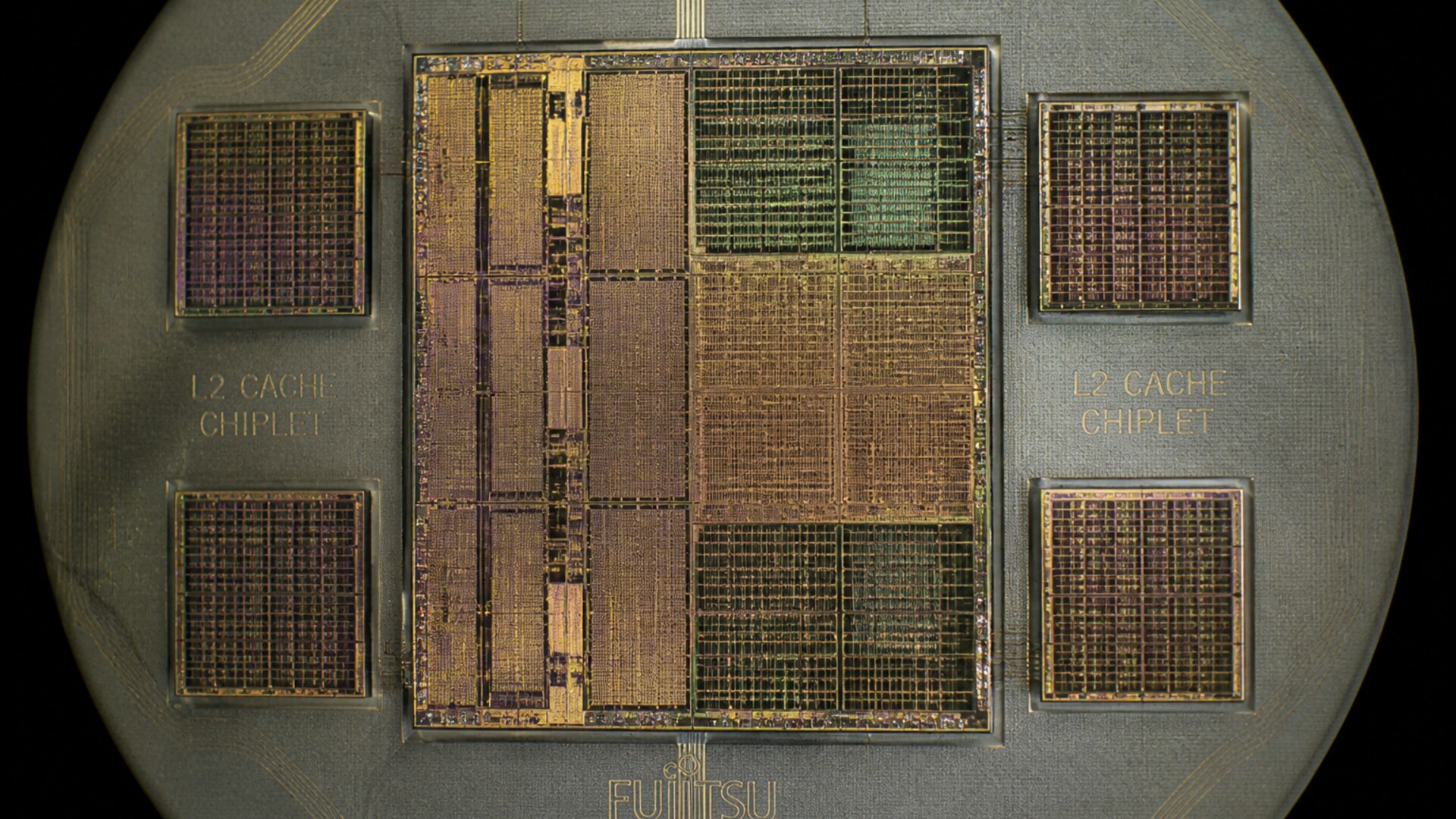
NUMA can be 1, 4, or 8 nodes — 144, 36, or 18 cores. ServeTheHome filed the 1-node layout for large-memory work and the 8-node layout for throughput. Each NUMA node can split into two LLC regions. Fujitsu lists up to 63 MPAMs, independent of the NUMA cut. Chips and Cheese described a hub-and-spoke: a 5 nm I/O die, 2 nm compute dies of 36 cores each, those compute dies stacked on 5 nm cache dies. Four compute dies at 36 cores is 144. In the 8-node mode each compute die splits in two, 18 cores and a private half of the L3 on the base die, because some cores sit closer to some of that cache. Fujitsu has not published L3 capacity. Chips and Cheese said so. The missing number stays missing. The macro photograph is the cache argument in metal: a central die, four square satellites, L2 CACHE CHIPLET printed on the substrate, FUJITSU at the bottom of the circle.
Fujitsu's table lists the 500 W part at 6,013 GFLOPs DGEMM and 96.2 TOPS INT8 at base, the 350 W part at 4,355 GFLOPs and 69.7 TOPS. Both parts are rated around 500 GB/s in STREAM Triad. The company claims up to 2× AI performance and more than 50 percent TCO reduction against unnamed comparisons. Keep the comparisons unnamed. Ultra-low-voltage operation is the efficiency paragraph: the core around 30 percent below nominal voltage for roughly half the power, which is how 144 cores fit in 350 W. Okazaki called that "energy saving comparable to moving one generation beyond the 2 nanometers," done with custom SRAM and a proprietary CAD flow for non-standard low voltage. Those are Fujitsu estimates until a 2027 lab run. Ian Cutress of More Than Moore asked about core-to-core latency with dies on opposite sides of the package and traffic through the I/O die. Fujitsu pointed at the face-to-face hybrid bonding and declined to give a latency figure.
NEDO subsidises Monaka under a green data-centre programme aimed at 40 percent energy savings by 2030. The 2 nm and 5 nm dies still come from TSMC. Tom's Hardware noted the gap between a made-in-Japan design and Taiwanese wafers, against Japan's more than 2 trillion yen for Rapidus 2 nm in Hokkaido by 2027 and about 1.2 trillion yen for TSMC's Kumamoto fabs. Monaka predates that domestic capacity. The successor does not. Monaka-X, later, is the 1.4 nm follow-on with Arm SME2 and NVLink Fusion on the roadmap. FugakuNEXT, the roughly US$750 million RIKEN system announced in August 2025 with Fujitsu and Nvidia, will pair that Monaka-X with Nvidia GPUs over NVLink Fusion. RIKEN targets more than 600 FP8 exaFLOPS in a 40 MW envelope and about 100 times Fugaku's application performance, operation around 2030. That is a 2030 machine. This piece is the 24 August chip: 144 cores, cache on 5 nm, samples now, volume 2027.
By 2027, 144 cores will sit in the middle of the Arm server field, not on top of it. AWS Graviton5 is 192 Neoverse V3 cores. Ampere's Aurora roadmap runs to 512. Microsoft Cobalt 200 is 132 cores with its own per-core DVFS. Monaka's separation is the cache-on-its-own-die stack and 12-channel DDR5, not a core-count trophy. The 256-bit SVE2 width matches SiPearl's Rhea1 and exceeds the 128-bit SVE2 common on hyperscaler Arm cores. Fujitsu has not changed the 144-core count, the node split, or the 2027 date across three years of disclosures since 2023. Okazaki's 24 August talk was the first time the dual 256-bit SVE2 and the entire last-level cache on a separate 5 nm die were said on a Hot Chips floor.
Broadcom's 3.5D XDSiP packaging is the name ServeTheHome and later coverage put on the hybrid-bond stack. The I/O die across the interposer is still 5 nm. The expensive 2 nm stays under 30 percent. That is the cost argument Okazaki was making on 24 August: do not spend N2P on SRAM that no longer shrinks, do not spend it on analog LDOs, spend it on the 144 cores that sit on the cool side of the bond. Two SKUs, both 144 cores, 350 W air at 2.1 GHz, 500 W liquid at 2.9 GHz. Twelve channels of DDR5. Ninety-six lanes of PCIe 6.0. Samples now. Volume 2027. The last-level cache is on a 5 nm die of its own. Fujitsu said so on a Hot Chips slide, and the photographs are the wafer and the package that make the slide a physical object.
The paper
Comments
No notes on this story yet.
Sign in to comment